
Voltage Glitching Unlocks Hidden Potential of Nvidia Mining Card
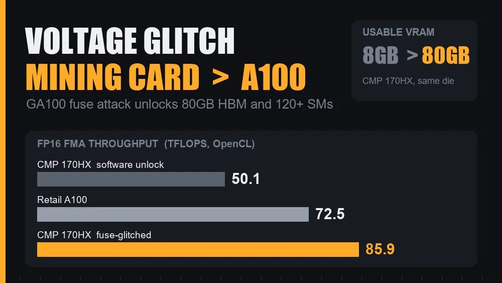
A hardware researcher known as Kate has published a detailed method to transform Nvidia's CMP 170HX mining card into a full-fledged 80GB A100-class accelerator using voltage fault injection. The mod, reported by Tom's Hardware and Hardware Busters on November 12, 2026, exploits the card's GA100 die—the same silicon used in Nvidia's flagship A100 data center GPU—to bypass fuse-based restrictions that Nvidia imposed to segment the product for the cryptocurrency mining market. According to the reports, the modified card not only matches but exceeds the FP16 throughput of a retail A100, achieving 85.9 TFLOPS compared to the A100's 72.5 TFLOPS.
The CMP 170HX was originally launched in 2021 as a mining-specific card with 8GB of usable memory, 70 streaming multiprocessors, PCIe Gen1, and no NVLink. However, Kate's research reveals that the 8GB model physically carries approximately 80GB of HBM2e memory on the package, with the extra capacity disabled via eFuses. By carefully glitching the fuse controller during boot, the hack unlocks the full memory and additional shader modules, resulting in a card that behaves like an A100 with 80GB VRAM. In a sample of ten 8GB cards, nine had the full 80GB intact, suggesting a high success rate for the hardware modification.
The Technical Trick: Glitching the Fuse Controller
The voltage glitching attack targets the GA100's fuse controller, which holds 16,384 eFuses used for yield control and product segmentation. These fuses include "fuseless fuses"—records that the controller replays at boot, with later records overriding earlier ones. Normally, the controller refuses to burn rows that would clear restrictions, but Kate's method bypasses this check by injecting precise voltage dips into the PWMVID line, which the GPU uses to communicate with its voltage regulator. A custom STM32G4-based board, designed with help from an AI model, feeds the MP2888B regulator a crafted waveform after removing a single 0402 resistor. By cycling the host PC through S3 sleep, the researcher generates repeated power-up sequences, and a card typically unlocks after one to 48 hours of glitching.
Once unlocked, the CMP dies usually have 120 to 126 working SMs, compared to the 108 SMs enabled in retail A100s. This explains the performance gain: with all SMs active, the card outperforms the A100 in raw FP16 compute, as measured by the ProjectPhysX OpenCL benchmark. The reports note that software-only unlockers had previously exposed 64GB on the 8GB model, but the fuse attack gets the remaining memory and shader modules.
Context: Why This Matters
The CMP 170HX was always an odd product, built on the same GA100 die as the A100 but fused down to serve miners during the Ethereum boom. As mining profitability declined, these cards became available on the secondary market at a fraction of their original cost—often around $2,500—while a full A100 with 80GB VRAM retails for upwards of $20,000. The voltage glitching hack thus represents a massive value proposition for those with the technical skills to perform the modification, effectively turning a cut-down mining card into a high-end AI accelerator.
This development also highlights the physical similarities between Nvidia's consumer and data center products, and the extent to which product segmentation is enforced through firmware and fuses rather than hardware differences. Similar to how wealthy investors flood into alternative assets as stocks and bonds lose their edge, hardware enthusiasts are finding unconventional ways to extract value from repurposed mining equipment.
Security and Ethical Implications
The ability to bypass fuse-based restrictions raises concerns about hardware security and the potential for counterfeit or modified cards to enter the market. Nvidia has not commented on the vulnerability, but the method underscores the risks of relying on eFuses for product segmentation. It also demonstrates the ingenuity of the modding community, which continues to find ways to repurpose hardware beyond its intended use.
While the hack requires physical modification and carries risks—such as bricking the card or causing permanent damage—the reports suggest that the procedure is reproducible and that the unlocked cards can outperform their retail counterparts. This could lead to a wave of modified CMP 170HX cards being sold on secondary markets, although buyers should be aware of the potential instability and lack of official support.
Perspective: Broader Trends in Hardware Hacking
The voltage glitching exploit is part of a larger trend of hardware enthusiasts and researchers finding innovative ways to unlock hidden capabilities in consumer and enterprise products. From BIOS mods to firmware exploits, the boundaries between product tiers are increasingly defined by software and firmware locks rather than physical hardware differences. This case is particularly notable because it targets a data center-grade GPU, blurring the line between mining cards and AI accelerators.
As AI workloads continue to grow, the demand for high-memory GPUs like the A100 remains strong, and cost-effective alternatives are highly sought after. The ability to convert a $2,500 mining card into an 80GB accelerator could disrupt the secondary market for A100s and similar GPUs, especially among startups and researchers with limited budgets. However, the technical complexity and risks involved mean that this hack is likely to remain a niche pursuit for skilled hardware hackers rather than a mainstream solution.
Nvidia's product segmentation strategy relies on both hardware and firmware locks, and this incident shows that determined individuals can circumvent those locks with enough effort. It remains to be seen whether Nvidia will respond with hardware revisions or legal measures, but for now, the cat-and-mouse game between manufacturers and modders continues.
Comments